

TSV technology used in new Samsung chip
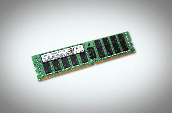
Samsung’s 128-gigabyte module. [SAMSUNG ELECTRONICS]
The TSV-based chip can significantly boost signal transmission and energy efficiency due to the structure. Conventional chip packages connect die stacks with wire bonding, while the TSV technology allows the dies to be stacked on top of one another through fine holes.
The latest DRAM module has the largest capacity and highest energy efficiency compared to any competing modules, according to Samsung.
The development follows the release of the world’s first 64-gigabyte 3-D DRAM product in 2014. Processing speed and storage have doubled with higher energy efficiency since then.
The 128-gigabyte module will be primarily used by enterprise-level users such as data centers.
“Mass production of the 128-gigabyte DRAM will help global IT players better manage their servers,” said Choi Joo-sun, executive vice president at Samsung Electronics’ memory sales and marketing division.
BY PARK EUN-JEE [park.eunjee@joongang.co.kr]


with the Korea JoongAng Daily
To write comments, please log in to one of the accounts.
Standards Board Policy (0/250자)