

Blaming the big companies
The author is the head of the industry 2 team at the JoongAng Ilbo.
The debate on risks from Japan’s export restrictions has found scapegoats in a strange place. Some in the government and ruling party are blaming large companies for their “shortsightedness and unpreparedness.” They raised questions why companies ranking globally in chip, display and smartphone production have neglected to groom the value chain in terms of small and mid-sized enterprises at home. They are implying that the imbalanced growth has made Korea’s core industry a point of weakness and an easy target for Japanese attack.
The accusation is not entirely wrong. Current difficulties wouldn’t have arrived if the Korean component industry grew hand in hand with materials. But that is not entirely the fault of Samsung Electronics and SK Hynix. Korea has become a powerhouse in semiconductors and displays through global distribution networks. The global IT industry has advanced through competition among companies raising the bar in innovation based on best possible materials and parts.
Take hydrogen fluoride (etching gas), one of the three materials singled out for exports restrictions by Japan. The etching gas is used to clean unnecessary chemicals off to refine patterns on the wafers for chips and displays. A high-purity form is employed on dynamic random access memory (DRAM) and flash memory chips. A less pure etching gas can be used in the fabrication of OLEDs, and low-purity hydrogen fluoride on liquid-crystal display (LCD) glass. Local hydrogen fluoride is already being tested by LG Display on LCD fab lines. LG Display is relatively more relaxed than the chipmakers not because it was ready, but because it is easier and less risky to make the product.
According to the Korea International Trade Association (KITA), Japanese made 43.9 percent of hydrogen fluoride imported into Korea from January to May. Annual shipments from Japan are worth less than 100 billion won ($84.9 million), but nevertheless the product is regarded as the best in the world. It is more cost efficient for a company to purchase the best available parts instead of investing in direct production. All chipmakers work that way.
Samsung Electronics and SK Hynix have the world’s largest capacity with over 300 fabs. But Japan and other countries excel in the essential equipment and materials needed for the fab process. For instance, the extreme ultraviolet lithography (EUV) system is the key to Samsung Electronics’ next-generation chip process. Dutch company ASML specializes in the machine, which costs 150 billion won per unit. Moving fast and buying the best tools and materials available has allowed Samsung Electronics to stay ahead in the cutting-edge competition. Samsung Electronics would never have made it to the top if it tried to control the entire chip-making process.
Finding replacements for the materials being restricted — fluorinated polyamides, photoresists and hydrogen fluoride — is working out. The output yield may have to be adjusted, but fab operators won’t likely have to stop the lines.
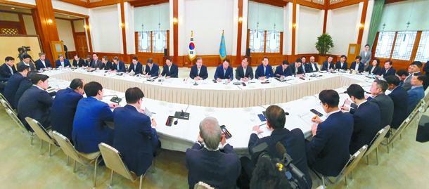
President Moon Jae-in on July 10 discusses with leaders of the 30 largest Korean companies how to cope with Japan’s restrictions on key materials used for semiconductors and displays. [YONHAP]
JoongAng Ilbo, July 24, Page 27


with the Korea JoongAng Daily
To write comments, please log in to one of the accounts.
Standards Board Policy (0/250자)