

HBM rivalry peaks with Micron in the game
![SK hynix's HBM3E chip, of which samples were shipped to Nvidia in August, 2023. [SK HYNIX]](https://koreajoongangdaily.joins.com/data/photo/2024/03/09/8a4f29ca-403b-4568-8b14-dbc79265f030.jpg)
SK hynix's HBM3E chip, of which samples were shipped to Nvidia in August, 2023. [SK HYNIX]
The American memory chipmaker said it will supply chips for Nvidia's upcoming H200 GPU in the second quarter, a feat that even Samsung hasn't achieved.
The announcement was a revolt from an underdog as the U.S. company barely held 10 percent of the global market last year.
The cutthroat competition became more evident when the Seoul court sided with SK hynix on Thursday by granting a noncompete injunction to prevent its former researcher, who specialized in HBM, from working at Micron. He would be fined 10 million won for each day in violation.
HBM has become essential in powering AI processors with its ability to process vast amounts of data faster than traditional dynamic random access memory (DRAM) can. Supplying it to Nvidia has become something of a holy grail among HBM producers as the U.S. GPU maker controls 90 percent of the AI chip market.
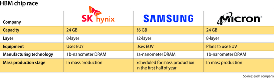
Micron's HBM3E will be made with 1b nanometer DRAM chips, which are par with 12-nanometer nodes, and which industry leader SK hynix is also using in its HBMs at the moment. The company is technologically ahead of Samsung, which still relies on 1a nanometer technology equivalent to 14-nanometer technology.
“It's proven that Micron's manufacturing method is more advanced than Samsung Electronics because their HBM3E will be made with 1b nanometer technology,” said chip expert Jeon In-seong, author of “The Future of the Semiconductor Empire.”
“Micron will need some more work in the packaging side, but that should be easier than what they've already achieved with 1b nanometer technology.”
SK hynix is cementing its leadership in the niche, yet profitable segment. It grabbed 54 percent of the HBM market last year, according to Goldman Sachs.
It is pouring 1.3 trillion won into Korea's advanced packaging facilities, this year alone, to ramp up its capacity to produce premium chips. Packaging has increasingly become important in advanced chips, including HBM, which integrates a vertical stack of multiple memory devices.
SK hynix was the first to equip its HBM with what's called MR-MUF (Mass Reflow-Molded Underfill) packaging technology, beginning in its third generation. The technology involves injecting liquefied protective material in between its stacked chips to protect the devices and prevent heat dissipation and is considered a core impetus behind SK hynix's current dominance in the space.
The company is the sole supplier of HBM3 chips for Nvidia's H100 processor. It is in the verification process for the supply of its HBM3E, which has entered initial mass production, for the H200.
“It will remain ahead of rivals in terms of client credibility and profitability,” Ko Young-min, an analyst at Daol Investment & Securities said in a note.
“Even if Micron attempts at the MR-MUF manufacturing technology, it will take some time to catch up with SK hynix considering the time and effort needed.”
Samsung Electronics catching up
Samsung has tumbled on a few rocks in the HBM race, but it is now catching up at full speed.
The company recently announced of its development of 12-layered HBM3E with capacity of 36GB — the industry's largest. SK hynix' and Micron's products have eight layers an 24GB capacity.
Samsung has started shipping samples to clients and hopes to enter mass production by the first half of this year.
It also continues wooing Nvidia.
Samsung is showcasing the 12-layered HBM3E chip at Nvidia's GPU Technology Conference 2024, which begins on March 18 in San Jose, California. The chipmaker will speak on its Compute Express Link technology, also known as CXL, which is an interface designed to boost the efficiency of processors.
It is making a speech there on Compute Express Link technology, also known as CXL, an open industry standard meant to improve both the performance and efficiency of CPUs.
“It is a hard game for Samsung because unless you have a big breakthrough in technology, it is hard to newly list as a supplier,” Jeong said. “But they just started ramping up their efforts in HBM, and it is a natural thing they don't see obvious progress just yet.”
BY JIN EUN-SOO [jin.eunsoo@joongang.co.kr]


with the Korea JoongAng Daily
To write comments, please log in to one of the accounts.
Standards Board Policy (0/250자)