

SK Hynix has a 96-layer NAND
96-layer CTF-based 4D NAND
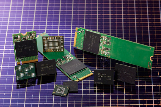
The new product is a 96-layer 512 gigabit (Gb) CTF-based 4D NAND flash, which SK Hynix claims to be the world’s first. A single chip offers 64 gigabytes of storage. Its mass production is set to start by the year’s end.
NAND flash is a non-volatile chip that does not require electricity to retain data that is used in consumer electronics like PCs, smartphones and servers. A larger number of layers offers more storage capacity.
Compared to the preceding 72-layer 512 Gb 3D NAND flash, the 96-layer chip is more than 30 percent smaller, which increases the number of chips on a wafer by 49 percent. The speed to write data was reduced by 30 percent and to read data by 25 percent. The data transfer speed was also accelerated to 1,200 megabits per second, which is around 30 percent faster than the 72-layer NAND flash.
“This 96-Layer CTF-based 4D NAND, with the industry’s top cost competitiveness and performance, will become a milestone in the company’s NAND flash business, as a platform in developing future products,” said Kim Jung-tae, vice president and head of NAND marketing at SK Hynix.
Another difference between the two models comes from the data storage method. SK Hynix has followed in the footsteps of Samsung Electronics and Toshiba to use Charge Trap Flash (CTF) technology for the new chip. CTF is a relatively new method of using silicon films to store data inside 3D chips. SK Hynix has taken it one step further by integrating a technology called Peri (short for peripheral circuit) Under Cell (PUC). The PUC can place a Peri, which controls cell operation, beneath the data-storing cells, adding an additional layer but creating more storage space. That led SK Hynix to add “4D” to the name of the new chip. Conventionally, Peris are placed alongside data-saving cells.
SK has become the third manufacturer to succeed in developing NAND flash with more than 90 layers. Samsung Electronics and Toshiba succeeded months earlier.
SK is relatively weaker in NAND as opposed to DRAM memory chips. A larger storage capacity with higher space efficiency is expected to reduce costs for both SK Hynix and its customers, the company explained.
“To achieve storage of 512 Gb, attaching two wafers of 256 Gb 3D NAND next to each another has been the most common method,” said an SK Hynix spokesman, “but with the new 96-layer 512 Gb, you can achieve the same level with a single wafer.”
The chip-making unit of Korea’s third-largest conglomerate plans to introduce 1-terabyte solid-state drives (SSDs) using its 96-layer 512 Gb 4D NAND Flash by the end of this year.
BY SONG KYOUNG-SON [song.kyoungson@joongang.co.kr]


with the Korea JoongAng Daily
To write comments, please log in to one of the accounts.
Standards Board Policy (0/250자)