

They can make it, but they don’t
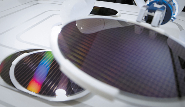
The manufacturing process for semiconductors incorporating quantum cryptography technology is demonstrated. [JOONGANG ILBO]
After two hours of fierce discussion, they concluded, yet again, they couldn’t. Just like six years ago.
“We are confident about our technology, but the hefty cost and high entry barrier still remain a problem,” said the company CEO, who only wanted to be identified as Kim.
For a small company with an annual revenue of around 10 billion won ($8.5 million), commercializing the technology is impossible, he added.
The company developed a technology to produce ultra-high purity hydrogen fluoride. It received a patent for the process in 2013. Filtering out impurities was key to the technology. This is done by getting hydrogen peroxide to bind to arsenic using ultra-sound.
According to the patent, the technology could refine hydrogen fluoride to a purity of 99.99999999 percent. Hydrogen fluoride from Japan is 99.999 percent pure.
“On top of costs and human resources additionally required, we won’t be able to handle the protests from the residents of the region we will be building a plant in. Obtaining permission isn’t easy, either,” the CEO said.
Material and equipment producers, even after developing certain technologies and applying for patents, have to overcome big and small barriers.
They have to secure pilot production lines, analysis equipment and pass several tests.
As the final stage, they have to pass mass production tests to become suppliers to Samsung Electronics or SK Hynix.
C&B Industrial estimates it will require up to 5 billion won to buy a metal analysis device and build a pilot production line.
To help smaller companies like C&B Industrial and to push the localization of materials, the government runs a few test centers, such as the Korea Advanced Nano Fab Center, the National Institute of Nanomaterials Technology and the National Nanofab Center.
The institutions allow researchers and developers to test materials or chip production devices. Some enable testing of 40-nanometer chips on 200 nanometer wafers.
But Samsung Electronics and SK Hynix already produce 7 nanometer to 14 nanometer chips using 300 nanometer wafers - much more advanced technologies.
“Chipmakers are waging a fierce competition at scaling down,” said Lee Jong-hee, director of the Korean Society of Semiconductors and Display Technology. “But the test equipment that smaller firms are able to use remains 10 to 15 years behind.”
According to the research by the society last year on 66 material and device producers, only four were equipped with facilities to test development of 300 nanometer wafers.
“If you want to be tested for Samsung and SK Hynix, developers are supposed to obtain a certificate of authorization from Belgium or the United States [due to the lack of local test facilities],” said an industry insider who asked to remain anonymous.
“As semiconductors make up a huge part of the Korean economy, we should foster local equipment and device producers,” said Yeom Geun-young, professor of advanced materials science and engineering at Sungkyunkwan University. “Initial-stage test facilities will be the priority for localizing chip-related materials.”
BY CHANG CHUNG-HOON [ebusiness@joongang.co.kr]


with the Korea JoongAng Daily
To write comments, please log in to one of the accounts.
Standards Board Policy (0/250자)