

Chip packaging is tech's new frontier — and Korea is lagging behind
Published: 05 Sep. 2024, 06:00
![Samsung Electronics Executive Chairman Lee Jae-yong, third from right, visits Samsung Electronics' chip packaging line in Cheonan, South Chungcheong, in February 2023. [YONHAP]](https://koreajoongangdaily.joins.com/data/photo/2024/09/05/5a399086-5518-46f7-95bf-f5c56dc948a2.jpg)
Samsung Electronics Executive Chairman Lee Jae-yong, third from right, visits Samsung Electronics' chip packaging line in Cheonan, South Chungcheong, in February 2023. [YONHAP]
Chip packaging — or the manufacturing of the casing that surrounds a semiconductor — has become a new battleground in the tech industry.
While the mounting of a chip may seem unimportant, it's a highly complex process crucial to the efficiency of AI and high-performance computing (HPC). The manner in which a chip is packaged impacts the flow of electricity into chips and facilitates its connection to the rest of the system, as well as aiding in cooling and damage protection.
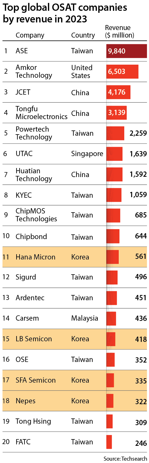
But while Korea may be a front-runner in memory chip manufacturing, the country lags significantly in advanced packaging technology, with domestic companies only taking up 4.3 percent of the global market.
As semiconductor scaling reaches its limit at 3 nanometers, advanced multichip packaging technology has become the key differentiating factor for cutting-edge innovation, particularly for use in the rapidly growing generative AI and HPC sectors.
The semiconductor industry will see a major shift, primarily for companies that generate value with advanced packaging, Boston Consulting Group said in a May report.
This is why China has been pouring state resources into localizing production for materials, parts and equipment and why Taiwan’s TSMC, the world’s largest foundry and a major player in advanced packaging, has tech firms like Nvidia and Apple lining up at its door.
It seems that Korea, in its current state, may become fodder for, not a forerunner of, this revolutionary shift.
The country’s share of the global chip packaging market slipped from 6 percent in 2021 to 4.3 percent in 2023, and shares of Nepes and Hana Micron, major domestic firms in the chip back-end business, dropped despite the semiconductor stock rally in the first half of this year.
“Korea’s high bandwidth memory chips are thought to be doing well, but all the advanced packaging that attaches them to AI semiconductors happens in Taiwan, and revenue for eight out of 10 domestic equipment businesses fell,” an executive in the materials, parts and equipment business said.
Korea’s two largest chip manufacturers, Samsung Electronics and SK hynix, rely on overseas products for 95 percent of the materials and equipment needed for advanced packaging, according to data compiled by the Ministry of Trade, Industry and Energy.
Collaboration needed for market leadership
Advanced packaging requires knowledge of materials’ chemical and electrical traits for fabrication, so tight collaboration between chip manufacturers and firms in the materials, parts and equipment industry is essential. But as Kang Sa-yoon, president of the Korean Microelectronics and Packaging Society, says, “domestic packaging firms are only fulfilling the development side, and not research, in R&D [research and development].”
A large number of domestic packaging firms rely on a small number of contractors — Samsung Electronics and SK hynix — for work, and, as such, are heavily affected by how well memory chips do and lack resources to invest in innovative technology.
“We have to invest in research for advanced packaging prior to clients’ requests as it would be too late to start when they do, but solely shouldering the risks, as a mid-sized business, is daunting,” said LB Semicon CEO Kim Nam-seok.
![Nvidia CEO Jensen Huang presents Nvidia's Blackwell platform at an event ahead of the Computex forum in Taipei, Taiwan in June. [REUTERS]](https://koreajoongangdaily.joins.com/data/photo/2024/09/05/53d7801d-b249-4baf-a3ef-4adaa9f2e359.jpg)
Nvidia CEO Jensen Huang presents Nvidia's Blackwell platform at an event ahead of the Computex forum in Taipei, Taiwan in June. [REUTERS]
It’s a different story in Taiwan, a region Nvidia CEO Jensen Huang praised for the rich ecosystem surrounding TSMC and advancements in packaging technology while promising continued partnerships with the region’s firms.
“In Taiwan, the world’s largest packaging firm, ASE, as well as small businesses, have dozens of clients; meanwhile domestic packaging firms rely on one contractor for even up to 70 to 90 percent of their revenue,” said Choi Bong-seok, author of “The Hidden Giants of the Semiconductor Industry” (2023).
“Only when economies of scale come into play, such as through multiple companies jointly securing contracts with overseas businesses, can proactive R&D be achieved in Korea,” the 20-year industry veteran added.
Experts also point out domestic chip firms’ limitations in horizontal cooperation, as they have historically achieved growth through vertical integration with a focus around their memory chip businesses.
“At Apple’s chip packaging meetings, employees from Taiwanese packaging firm ASE, printed circuit board manufacturer Unimicron and material production companies as well as those from Apple’s corporate headquarters participate. But in Korea, [contractors] merely hand out instructions,” an executive in the materials industry said.
![LB Semicon's semiconductor fabrication plant in Pyeongtaek, Gyeonggi [PARK HAE-LEE]](https://koreajoongangdaily.joins.com/data/photo/2024/09/05/7e374d47-061c-4caa-8704-2821182c190b.jpg)
LB Semicon's semiconductor fabrication plant in Pyeongtaek, Gyeonggi [PARK HAE-LEE]
Korean packaging fails to find place in global market
Key customers of advanced packaging include Big Tech firms such as Nvidia and Microsoft. The U.S. government has been taking advantage of the large demand to attract relevant technology to the country. SK hynix constructed an advanced packaging facility for HBM chips in Indiana and, in April, announced a $3.87 billion investment in an R&D partnership with Purdue University. Samsung Electronics is also considering making an advanced technology packaging line in Taylor, where the company’s second U.S. chip plant is currently being constructed.
Southeast Asia, meanwhile, has a stronghold in traditional packaging for legacy chips. Investment has been focused in countries including Malaysia and Vietnam after the China-U.S. conflict disrupted global supply chains.
Malaysian Prime Minister Anwar Ibrahim announced plans to allocate $5.3 billion to the country’s semiconductor industry, including funds to train 60,000 engineers in design, packaging and testing. The country expects the funds to further grow its 13 percent global market share in packaging, in line with its aim to become a “neutral and nonaligned” global chip hub. Intel already operates a new chip packaging and testing facility in Malaysia’s Penang created with a $7 billion investment.
![Nepes's semiconductor fabrication plant in South Chungcheong [NEPES]](https://koreajoongangdaily.joins.com/data/photo/2024/09/05/43c4d780-21d6-406c-b9e4-41a51207f9d1.jpg)
Nepes's semiconductor fabrication plant in South Chungcheong [NEPES]
With a long way to go in packaging technology advancements and traditional packaging work going to other countries, the regional economy and jobs in Chungcheong, where domestic packaging firms are clustered, anticipate turmoil.
“Global semiconductor supply chains are changing in the complete opposite direction of what we want,” a domestic packaging firm’s head said.
“Korean traditional packaging is losing its competitiveness in the market in terms of costs such as labor expenses; we must, therefore, invest in advanced packaging,” said Lee Byoung-hun, a professor at Pohang University of Science and Technology’s Department of Semiconductor Engineering.
The issue of space and human resources also has to be resolved to strengthen domestic packaging.
TSMC acquired a factory in Tainan, Taiwan, in July, with plans to expand its advanced packaging there. The factory is in proximity to Southern Taiwan Science Park, where advanced integrated circuits are produced.
In Korea, on the other hand, it is difficult to secure locations for clean rooms in Hwaseong, Yongin and Pyeongtaek in Gyeonggi, where many semiconductor fabrication plants are located, due to various regulations. Relocating to the countryside could potentially incur labor shortages.
Many Samsung Electronics researchers reportedly left for firms located in the Seoul metropolitan area after the company relocated its advanced packaging operations to Cheonan, South Chungcheong.
“There are employees who immediately quit after coming for their training and seeing that the factory is located in the middle of nowhere,” an employee of a packaging firm in South Chungcheong said. “Infrastructural support from the government, not just from individual companies, is necessary for younger people to live in the countryside.”
BY SHIM SEO-HYUN, PARK HAE-LEE [kim.juyeon2@joongang.co.kr]


with the Korea JoongAng Daily
To write comments, please log in to one of the accounts.
Standards Board Policy (0/250자)