

[Video] Chip war between Samsung and TSMC
Published: 16 Dec. 2020, 14:16
Updated: 16 Dec. 2020, 14:27
If there was a nuclear arms race during the cold war, now we are witnessing an arms race in silicon chips. Big chipmakers like TSMC have announced billions of dollars of new investment, and others are opting for massive mergers and acquisitions.
Samsung Electronics, which is the world’s biggest memory chipmaker, is also in the race. $121 billion has been pledged so it becomes the No.1 player in what it calls non-memory sector.
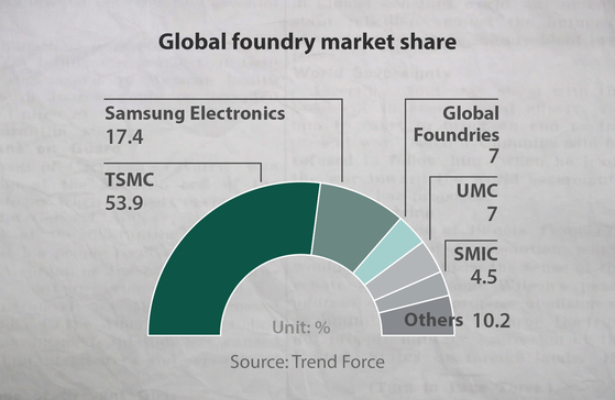
The ultimate competitor is Taiwan’s TSMC, as it is the top supplier with a dominant market share in that field.
We will pin down Samsung’s strategies in this battle and why it matters to you.
What is the Samsung Electronics chief strategy for the non-memory business?
Before we jump into the strategy, we need to talk about what the non-memory business exactly is. The term is more frequently used by the Korean press and chipmakers to indicate the chips other than memory chips. So they include central processing units for computers, application processors for smartphones and camera sensors.
The area also includes what is called foundry, which means building the microprocessors by contract based on the designs from outside customers.
As I mentioned before, Samsung is the largest manufacturer of memory chips, but its portion in foundry business is less than a third of the market share of TSMC.
To close the gap, Samsung will invest $121 billion into non-memory sector by 2030, proclaiming that it will become the top player in the sector.
A lot of that will be used to develop more advanced chip manufacturing processes, and the essence of that process is to shrink the node size.
Samsung and TSMC currently use 5-nanometer processes or above as the two are the only chipmakers capable of achieving the size. Both are planning to introduce 3-nanometer process in 2022.
What is the significance and impact of adopting 3-nanometer chips?
So you now understand Samsung is not “the player” in the playground.
But Samsung wants to shake off that image when it comes to release speed and functionality. TSMC was several months or at least a quarter ahead in mass producing a new generation of chip based on smaller node sizes.
For instance, it began mass-producing 7-nanometer chips in the second quarter of 2018, while Samsung got there in the first quarter in 2019. The gap narrowed for 5-nanometer chips, with TSMC releasing them in the first half of this year and Samsung in the third quarter.
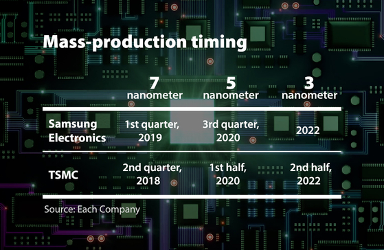
For the planned 3-nanometer product, the gap will be further narrowed in since the two chipmakers appear to be targeting end-2022 as the time for mass-production.
TSMC went more specific to say the second half of 2022, while Samsung only mentioned the year.
The Korean tech company should also prove technical advancement in the development of 3-nanometer chips because it plans to use a new technology called Gate-All-Around FET ahead of TSMC.
The technique is designed to enhance power density of the chips and thus improve energy efficiency, as the new design allows for more expanded and flexible current flows across channels at transistor gate compared to the widely used finFET technique.
TSMC said it will use the technique for the 2-nanometer chips.
More generally, Samsung would also be able to cut the production cost with smaller processes.
Why does the nanometer size matter?
You might have a sense that all the chip makers are obsessed with that nanometer size as you can see in tons of press releases marking the progress in their node size.
It is important because the process size is directly linked with the chip’s performance. The chip manufacturing process is like placing as many people as possible in a schoolyard to get something done. So, a wafer – a thin disc-shaped piece silicon – can be described as a schoolyard and transistors as people.

So, we can say that putting as many transistors on a wafer helps increase performance of an end chip product, and this is why transistor density should go up for better performance.
And the node size refers to the distance between transistors on a chip. The smaller the number, the more high-performing the chips while consuming less energy.
The chips using the 7-nanometer process have approximately 130 to 230 million transistors per square millimeter.
What is the benefit of the 3-nanometer chip from the consumer perspective?
The introduction of the new generation chip is more about improving the processing speed and energy consumption of electronic devices than enabling new services that we’ve never experienced before.
The better performance could be experienced on electronic devices with the 3-nanometer chip — including smartphones, tablets and laptops.
Technically, the smaller node size could provide the end product in smaller sizes.
But those in the semiconductor industry said that the difference is not significant enough to be felt by consumers, since the chips that we are using now are already miniscule.
BY PARK EUN-JEE [park.eunjee@joongang.co.kr]
VIDEO BY JEON TAE-GYU [jeon.taegyu@joongang.co.kr]


with the Korea JoongAng Daily
To write comments, please log in to one of the accounts.
Standards Board Policy (0/250자)